无机材料学报 ›› 2024, Vol. 39 ›› Issue (2): 129-144.DOI: 10.15541/jim20230453 CSTR: 32189.14.10.15541/jim20230453
所属专题: 【信息功能】柔性材料(202409); 【信息功能】MAX层状材料、MXene及其他二维材料(202409)
万胡杰1,2( ), 肖旭1()
收稿日期:2023-10-05
修回日期:2023-12-23
出版日期:2023-12-25
网络出版日期:2023-12-25
通讯作者:
肖 旭, 研究员. E-mail: xuxiao@uestc.edu.cn作者简介:万胡杰(1998-), 男, 博士研究生. E-mail: 202211022617@std.uestc.edu.cn
基金资助:
WAN Hujie1,2(), XIAO Xu1()
Received:2023-10-05
Revised:2023-12-23
Published:2023-12-25
Online:2023-12-25
Contact:
XIAO Xu, professor. E-mail: xuxiao@uestc.edu.cnAbout author:WAN Hujie (1998-), male, PhD candidate. E-mail: 202211022617@std.uestc.edu.cn
Supported by:摘要:
开发新型低维材料在太赫兹电磁屏蔽与吸收领域的应用是一个极为重要的研究方向, 低维材料以其独特的电学、力学与电磁响应而有望创造出更加高效的电磁屏蔽与吸收方案。二维过渡金属碳化物、氮化物与碳氮化合物MXenes在低频波段已经展示出优异的电磁屏蔽与吸收性能, 尤其是MXenes兼具高电导率、低密度、高柔性等特点, 有利于未来太赫兹器件便携化与系统集成化。然而, 将MXenes太赫兹电磁屏蔽与吸收材料推向实际应用过程中, 面临着附着稳定性、环境稳定性、不耐高温等问题, 无法满足航空航天和第六代通信场景需求。此外,目前缺乏更加全面的太赫兹散射与吸收验证手段。针对上述问题,研究人员开展了广泛且深入的工作。本文回顾了近年来主流电磁屏蔽与吸收材料的主体构型与基础理论原理, 并重点介绍了多种MXenes及其复合物在薄膜与多孔结构下的太赫兹电磁屏蔽与吸收特性, 包括Ti3C2Tx、Mo2Ti2C3Tx、Mo2TiC2Tx、Nb4C3Tx、Nb2CTx, 并展望了MXenes作为太赫兹频段中电磁屏蔽与吸收材料所面临的挑战和机遇。
中图分类号:
万胡杰, 肖旭. MXenes及其复合物的太赫兹电磁屏蔽与吸收[J]. 无机材料学报, 2024, 39(2): 129-144.
WAN Hujie, XIAO Xu. Terahertz Electromagnetic Shielding and Absorbing of MXenes and Their Composites[J]. Journal of Inorganic Materials, 2024, 39(2): 129-144.
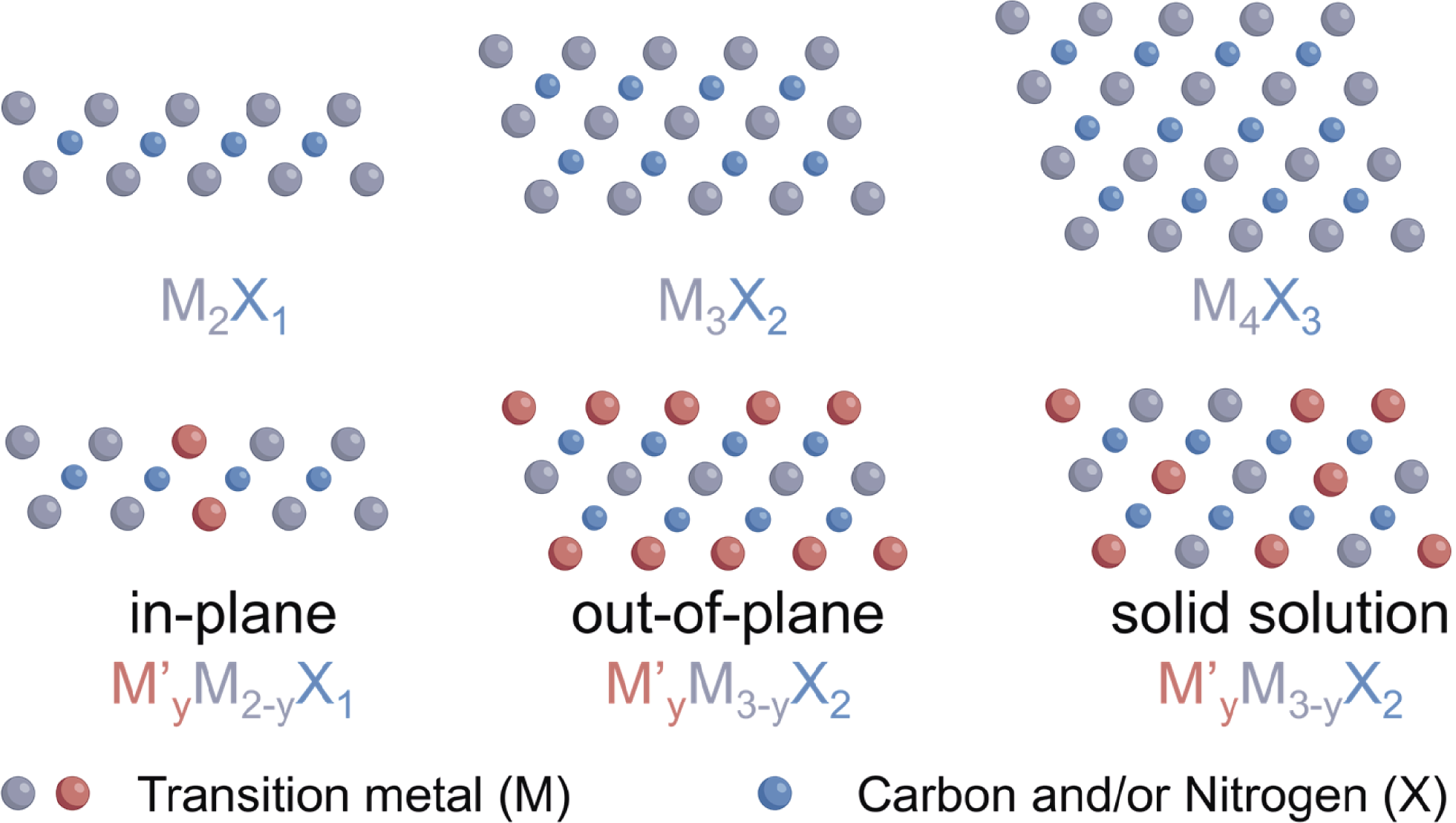
图1 MXenes的结构示意图
Fig.1 Chemical structures of MXenes 2D MXenes have a general formula of Mn+1XnTx, where M is an early transition metal, X is carbon and/or nitrogen, and Tx represents surface terminations of the outer metal layers. The n value in the formula can vary from 1 to 4, depending on the number of transition metal layers (and carbon and/or nitrogen layers) present in the structure of MXenes, for example, Ti2CTx (n = 1), Ti3C2Tx (n = 2), Nb4C3Tx (n = 3), and (Mo,V)5C4Tx (n = 4)
| Classification | Absorbing mechanism | Remark | |
|---|---|---|---|
Salisbury screen | A resistive sheet is placed | (a) Narrow band (b) Destructive interference (c) Easy to process | |
Jaumann absorber | The Jaumann absorber, an extension of the Salisbury screen, primarily comprises multiple thin impedance layers, lossless dielectric layers, and a metal layer. The electromagnetic characteristics of each impedance layer and the thickness of the dielectric layer are designed to operate at distinct frequencies, enabling destructive interference absorption across multiple frequency points and achieving broadband absorption. | (a) Broadband frequency (b) Destructive interference (c) Substantial thickness and intricate processing methods | |
Dällenbach absorber | The impedance matching layer is designed for specific high imaginary part of dielectric constant and permeability, while matching the free-space impedance. | (a) High imaginary part of dielectric constant and permeability (b) Free-space impedance matching (c) The absorption bandwidth is related to the conduction-frequency characteristics (d) Easy to process | |
| Classification | Absorbing mechanism | Remark | |
Impedance gradient multilayer absorber | Similar to the Dällenbach absorber, the layer-by-layer impedance matching design minimizes the reflected component of the interface when waves are incident. | (a) Gradient interface impedance matching (b) The absorption bandwidth is related to the conduction- frequency characteristics (c) Complicated process | |
Pyramidal type absorber | The pyramidal-type absorber, an evolution from the Dällenbach absorber framework, adopts a specific angle design to maximize incident wave capture, minimizing reflection. Electromagnetic waves undergo multiple reflections along the cone structure. Both pyramidal and tetrahedral pyramidal configurations exhibit reduced demands concerning the polarization direction of electromagnetic waves. | (a) The macrostructure captures the incident wave and reduces scattering (b) The absorption bandwidth is related to the conduction- frequency characteristics (c) Easy to process | |
Metamaterial absorber | The resonant response exhibited by distinctive metamaterial structure serves the purpose of dissipating incident electromagnetic waves. Owing to the notably high degree of freedom within this characteristic structure, metamaterials can be engineered for either single-frequency or wide-band resonant absorption. To achieve broadband absorption, multiple distinct single-frequency resonant structures are employed and combined. However, due to practical limitations in the manufacturing process, there remains a gap in absorption between the multiple resonant frequencies, leading to partial absorption within specific frequency bands. | (a) Electromagnetic resonance characteristic structure (b) Adjustable electromagnetic parameters ( (c) The processing difficulty is related to the wavelength | |
Coherent perfect absorber | When two normal incidence plane waves with an odd times π phase difference enter the impedance layer from both ends, interference cancelation occurs, and all electromagnetic waves will be absorbed. | (a) Coherent wave (b) Phase difference: (c) The absorption bandwidth is related to the conduction- frequency characteristics | |
Artificial blackbody | In the domain of artificial black holes, spheres and cylinders stand as prevalent design frameworks. Multi-layer spheres and cylinders are designed to increase the dielectric constant of the medium layer by layer from the outside to the inside. The center is full of material with high imaginary part of dielectric constant, and the incident wave is deflected to the center layer by layer and converges and loses. | (a) Gradient dielectric constant (b) The overall geometry is larger than the wavelength diffraction limit | |
表1 太赫兹电磁屏蔽与吸收机制[37-38]
Table 1 Terahertz electromagnetic shielding and absorption mechanism[37-38]
| Classification | Absorbing mechanism | Remark | |
|---|---|---|---|
| Salisbury screen | A resistive sheet is placed | (a) Narrow band (b) Destructive interference (c) Easy to process | |
| Jaumann absorber | The Jaumann absorber, an extension of the Salisbury screen, primarily comprises multiple thin impedance layers, lossless dielectric layers, and a metal layer. The electromagnetic characteristics of each impedance layer and the thickness of the dielectric layer are designed to operate at distinct frequencies, enabling destructive interference absorption across multiple frequency points and achieving broadband absorption. | (a) Broadband frequency (b) Destructive interference (c) Substantial thickness and intricate processing methods | |
| Dällenbach absorber | The impedance matching layer is designed for specific high imaginary part of dielectric constant and permeability, while matching the free-space impedance. | (a) High imaginary part of dielectric constant and permeability (b) Free-space impedance matching (c) The absorption bandwidth is related to the conduction-frequency characteristics (d) Easy to process | |
| Classification | Absorbing mechanism | Remark | |
| Impedance gradient multilayer absorber | Similar to the Dällenbach absorber, the layer-by-layer impedance matching design minimizes the reflected component of the interface when waves are incident. | (a) Gradient interface impedance matching (b) The absorption bandwidth is related to the conduction- frequency characteristics (c) Complicated process | |
| Pyramidal type absorber | The pyramidal-type absorber, an evolution from the Dällenbach absorber framework, adopts a specific angle design to maximize incident wave capture, minimizing reflection. Electromagnetic waves undergo multiple reflections along the cone structure. Both pyramidal and tetrahedral pyramidal configurations exhibit reduced demands concerning the polarization direction of electromagnetic waves. | (a) The macrostructure captures the incident wave and reduces scattering (b) The absorption bandwidth is related to the conduction- frequency characteristics (c) Easy to process | |
| Metamaterial absorber | The resonant response exhibited by distinctive metamaterial structure serves the purpose of dissipating incident electromagnetic waves. Owing to the notably high degree of freedom within this characteristic structure, metamaterials can be engineered for either single-frequency or wide-band resonant absorption. To achieve broadband absorption, multiple distinct single-frequency resonant structures are employed and combined. However, due to practical limitations in the manufacturing process, there remains a gap in absorption between the multiple resonant frequencies, leading to partial absorption within specific frequency bands. | (a) Electromagnetic resonance characteristic structure (b) Adjustable electromagnetic parameters ( (c) The processing difficulty is related to the wavelength | |
| Coherent perfect absorber | When two normal incidence plane waves with an odd times π phase difference enter the impedance layer from both ends, interference cancelation occurs, and all electromagnetic waves will be absorbed. | (a) Coherent wave (b) Phase difference: (c) The absorption bandwidth is related to the conduction- frequency characteristics | |
| Artificial blackbody | In the domain of artificial black holes, spheres and cylinders stand as prevalent design frameworks. Multi-layer spheres and cylinders are designed to increase the dielectric constant of the medium layer by layer from the outside to the inside. The center is full of material with high imaginary part of dielectric constant, and the incident wave is deflected to the center layer by layer and converges and loses. | (a) Gradient dielectric constant (b) The overall geometry is larger than the wavelength diffraction limit | |
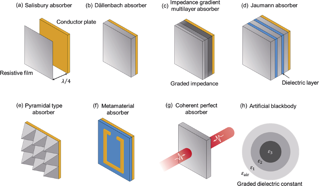
图2 典型电磁吸收体的原理示意图
Fig. 2 Schematic illustration of electromagnetic absorber (a) Salisbury screen absorber. The resistive film placed at 1/4 wavelength in front of the metal plate[39]; (b) Dällenbach absorber. The impedance of resistive film is equal to free space impedance to reduce reflection[38]; (c) Impedance gradient multilayer absorber. The impedance decreases layer by layer from large to small, reducing reflections while increasing conductive loss absorption[38]; (d) Jaumann absorber. All the layers are designed to operate at different wavelengths, so that the distance between each sheet is approximately
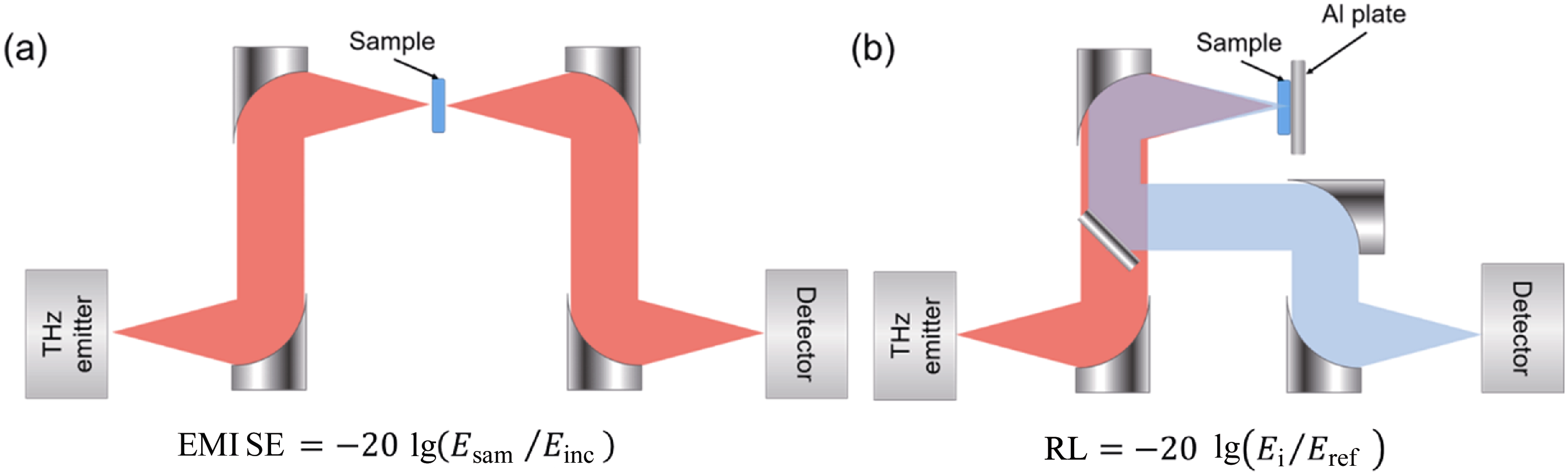
图3 太赫兹电磁屏蔽效能(a)和反射损耗(b)测试原理图[57]
Fig. 3 Schematic illustration of a THz-TDS system for electromagnetic interference shielding efficiency (a) and reflection loss measurements (b)[57] (Reprinted from Ref. [57] with permission, Copyright 2021, American Chemical Society)
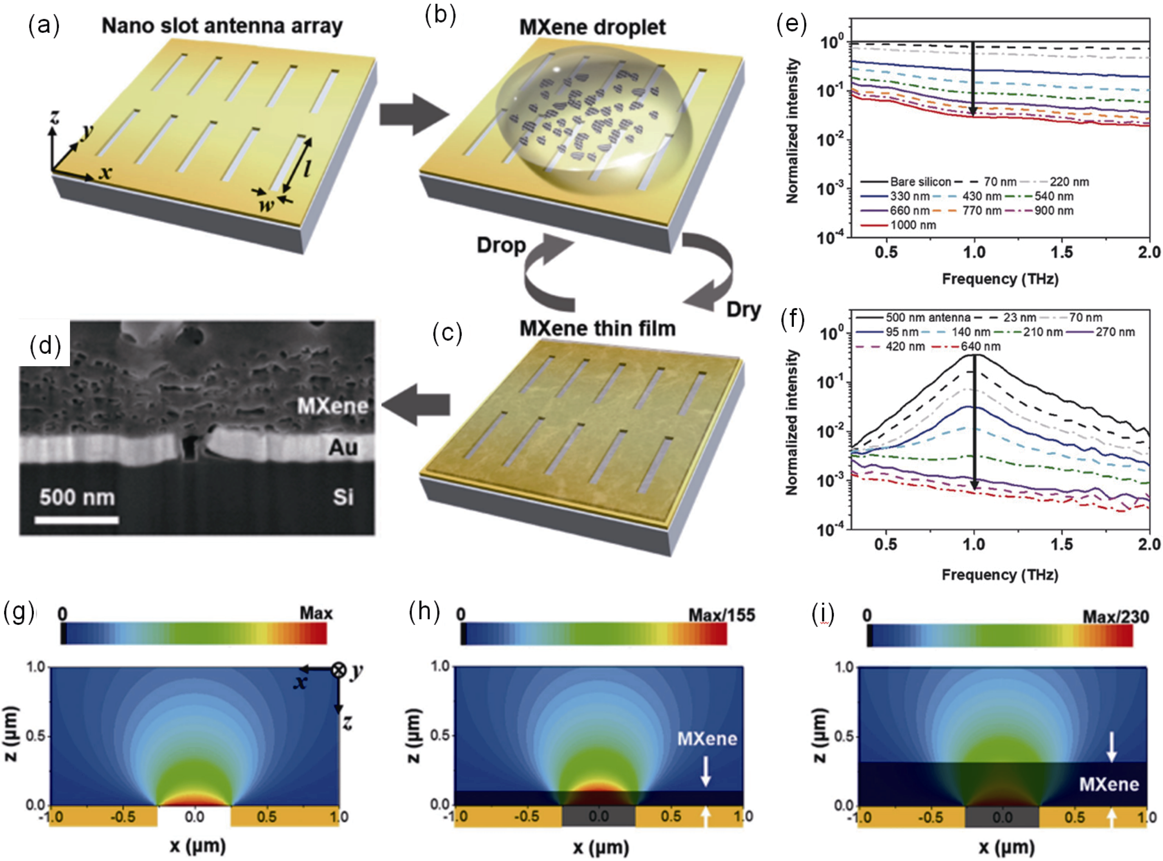
图4 基于金纳米狭缝天线的MXene电磁屏蔽增强现象[59]
Fig. 4 Enhanced THz electromagnetic shielding phenomenon of MXene based on gold nano-slit antenna[59] (a) Scheme of MXene-coated nano-metamaterial antennas; (b, c) Thin film of MXene made by drop-casting of MXene flakes followed by drying in air for many cycles to achieve the desirable thickness; (d) SEM image of the as-prepared MXene film with 150 nm width antenna; (e) Normalized transmittance spectra of the bare silicon and various thicknesses of MXene films on the silicon substrate; (f) Normalized transmittance spectra of the antenna and various thicknesses of MXene on the 500 nm width antenna array; Electric field intensity distributions of transmitted THz wave near the 500 nm width antenna, obtained by analytical calculation of antenna (g) without MXene, with (h) 100 nm thick MXene on the antenna and (i) 300 nm thick MXene on the antenna. The yellow and gray colors indicate the gold nano-slot antenna and MXene, respectively. In (h, i), the MXene filled the gap of the nano-antenna (Reprinted from Ref. [59] with permission, Copyright 2018, WILEY-VCH Verlag GmbH & Co. KGaA, Weinheim)

图5 MXenes的太赫兹电导响应特性
Fig. 5 Terahertz conductivity characteristics of MXenes (a) Complex THz conductivity of the 16 nm Ti3C2Tx film, and lines-global fitting of the real and imaginary conductivity to the Drude-Smith model (solid red line, fit to σ1, dashed blue line, fit to σ2)[60]; (b) Schematic representation of a Ti3C2Tx film: five atomic layers thick Ti3C2 cores of individual flakes are terminated by -OH, -F, or =O groups; (c) 2 μm by 2 μm AFM micrograph of a 25 nm thick Ti3C2Tx film; (d) THz spectroscopy experiment; (e) THz probe pulse transmitted through the substrate with a Ti3C2Tx film; (f) Corresponding THz electric field amplitude; (g) THz complex conductivity (solid symbols represent real and open symbols represent imaginary conductivity components; lines show a global fit of both components to the Drude-Smith model); (h) EMI SE calculated from data in (e)[62]; (i) Terahertz conductivity of Nb4C3Tx and Ti3C2Tx MXene thin films; (j) Real component of THz conductivity in three MXenes films (Ti3C2Tx, Mo2Ti2C3Tx and Nb2CTx) measured by the THz time-domain spectroscopy. Symbols are experiment data, and lines are fit to the Drude-Smith model. Extrapolation 0 THz yield static, DC conductivity[63-64]; TDS of (k, l) Mo2Ti2C3Tz and (m, n) Mo2TiC2Tx (k, m) as deposited and (l, n) after a mild 200 ℃ vacuum annealingz. Solid symbols represent real and open symbols represent imaginary conductivity, with lines showing global fits of both the real and imaginary conductivity to the Drude-Smith model with parameters σDC, τDS and c indicated on individual panels[61] (Reprinted from Ref. [60] with permission, Copyright 2022, IOP Publishing; Reprinted from Refs. [61-62] with permission, Copyright 2020, American Chemical Society; Reprinted from Ref. [63] with permission, Copyright 2022, Wiley-VCH.; Reprinted from Ref. [64] with permission, Copyright 2022, Springer Nature)
| MXenes | Film fabrication method | Thickness/nm | c | Ref. | |
|---|---|---|---|---|---|
| Ti3C2Tx (MILD) | Interfacial thin film technology | 16 | 6±1 | -0.97±0.03 | [ |
| Ti3C2Tx (MILD) | Interfacial thin film technology | 25±5 | 19±1 | -0.68 | [ |
| Ti3C2Tx | / | / | 67±3 | ~ -0.65 | [ |
| Al-Ti3C2Tx | Self-assemble technology | 3.0±0.2 | 9.62±0.1 | -0.82±0.0015 | [ |
| 6.4±0.3 | 10.61±0.2 | -0.79±0.0016 | |||
| 8.0±0.7 | 10.73±0.2 | -0.76±0.0019 | |||
| 10.2±0.1 | 10.98±0.2 | -0.72±0.0016 | |||
| 11.8±0.5 | 12.60±0.2 | -0.68±0.0013 | |||
| 13.3±0.5 | 12.59±0.1 | -0.66±0.0012 | |||
| Mo2Ti2C3Tx (HF TBAOH) | Spin-coating technology | ~80 | 16±3 | -0.941±0.007 | [ |
| Annealing-Mo2Ti2C3Tx (HF TBAOH) | Spin-coating technology | ~80 | 20±4 | -0.875±0.013 | [ |
| Mo2TiC2Tx (HF TBAOH) | Drop-cast technology | ~1300 | 36±4 | -0.864±0.007 | [ |
| Annealing-Mo2TiC2Tx (HF TBAOH) | Drop-cast technology | ~1300 | 31±3 | -0.895±0.005 | [ |
| Nb4C3Tx-few layer (HF TMAOH) | / | / | 52±4 | ~ -0.7 | [ |
表2 MXenes基于Drude-Smith模型的太赫兹电子弛豫时间与背散射拟合参数[60⇓-62,64 -65]
Table 2 MXenes fitting parameters for terahertz electron relaxation time and backscattering based on the Drude-Smith model [60⇓-62,64-65]
| MXenes | Film fabrication method | Thickness/nm | c | Ref. | |
|---|---|---|---|---|---|
| Ti3C2Tx (MILD) | Interfacial thin film technology | 16 | 6±1 | -0.97±0.03 | [ |
| Ti3C2Tx (MILD) | Interfacial thin film technology | 25±5 | 19±1 | -0.68 | [ |
| Ti3C2Tx | / | / | 67±3 | ~ -0.65 | [ |
| Al-Ti3C2Tx | Self-assemble technology | 3.0±0.2 | 9.62±0.1 | -0.82±0.0015 | [ |
| 6.4±0.3 | 10.61±0.2 | -0.79±0.0016 | |||
| 8.0±0.7 | 10.73±0.2 | -0.76±0.0019 | |||
| 10.2±0.1 | 10.98±0.2 | -0.72±0.0016 | |||
| 11.8±0.5 | 12.60±0.2 | -0.68±0.0013 | |||
| 13.3±0.5 | 12.59±0.1 | -0.66±0.0012 | |||
| Mo2Ti2C3Tx (HF TBAOH) | Spin-coating technology | ~80 | 16±3 | -0.941±0.007 | [ |
| Annealing-Mo2Ti2C3Tx (HF TBAOH) | Spin-coating technology | ~80 | 20±4 | -0.875±0.013 | [ |
| Mo2TiC2Tx (HF TBAOH) | Drop-cast technology | ~1300 | 36±4 | -0.864±0.007 | [ |
| Annealing-Mo2TiC2Tx (HF TBAOH) | Drop-cast technology | ~1300 | 31±3 | -0.895±0.005 | [ |
| Nb4C3Tx-few layer (HF TMAOH) | / | / | 52±4 | ~ -0.7 | [ |
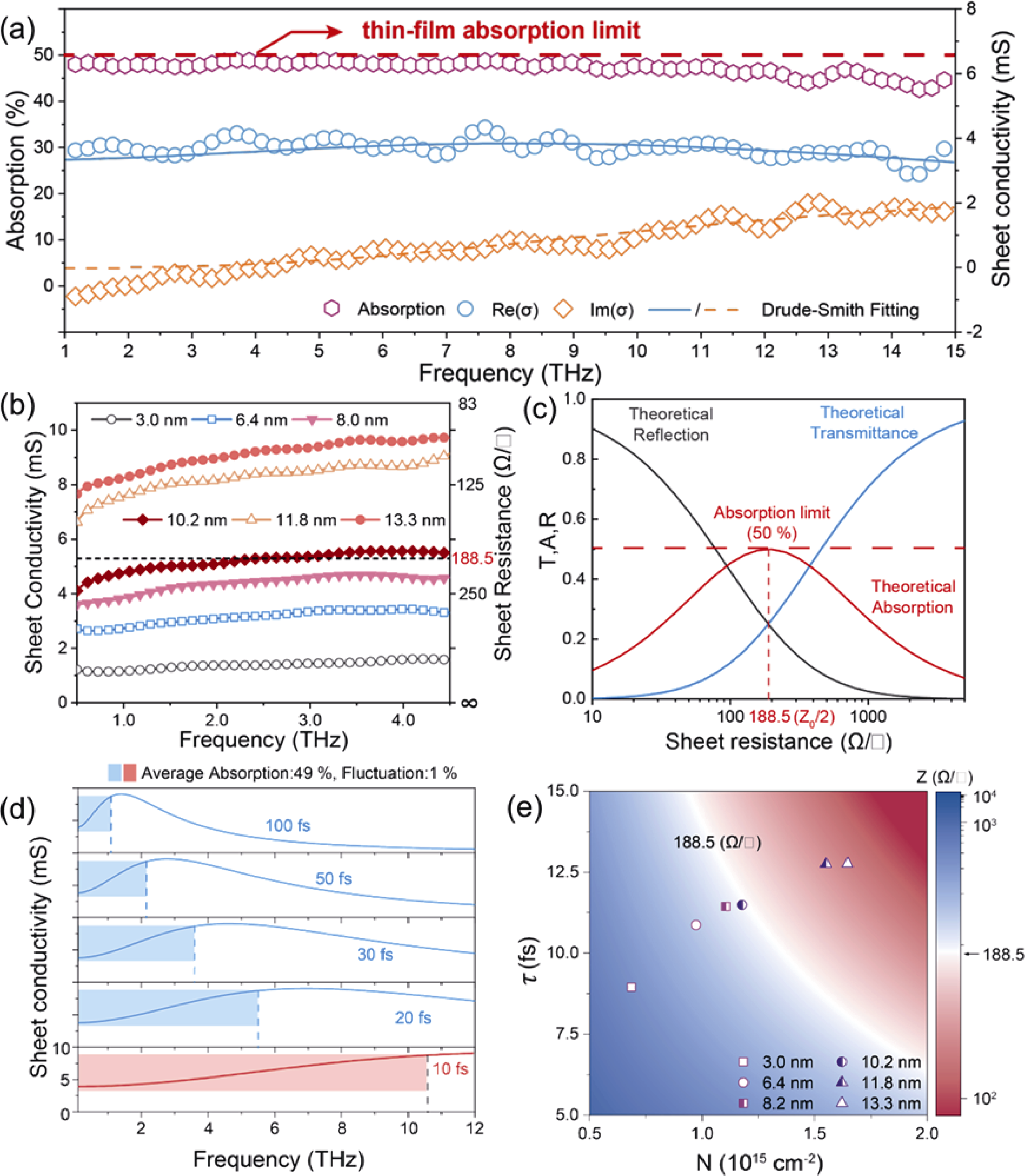
图6 自组装Ti3C2Tx薄膜的层数依赖太赫兹响应特性[65]
Fig. 6 Layer-dependent terahertz (THz) conductivity observed in self-assembled Ti3C2Tx films[65] (a) Ultrabroadband terahertz absorption and conductivity of a 17.2 nm Ti3C2Tx film measured by an air plasma-based THz-TDS system; (b) Terahertz sheet conductivity and resistance of Ti3C2Tx assemblies with different thicknesses for 0.5-4.5 THz; (c) Theoretical transmittance, reflectance and absorption simulated by impedance theory; (d) Conductivity as a function of frequency for a Drude-Smith model with different relaxation times. The shaded bars show the regions where the average absorption is 49% and fluctuation is 1%; (e) Relaxation time τ and sheet carrier concentration N for Ti3C2Tx assemblies with different thicknesses. The blue and red colours indicate the higher and lower impedance, respectively (Reprinted from Ref. [65] with permission, Copyright 2023, Springer Nature)
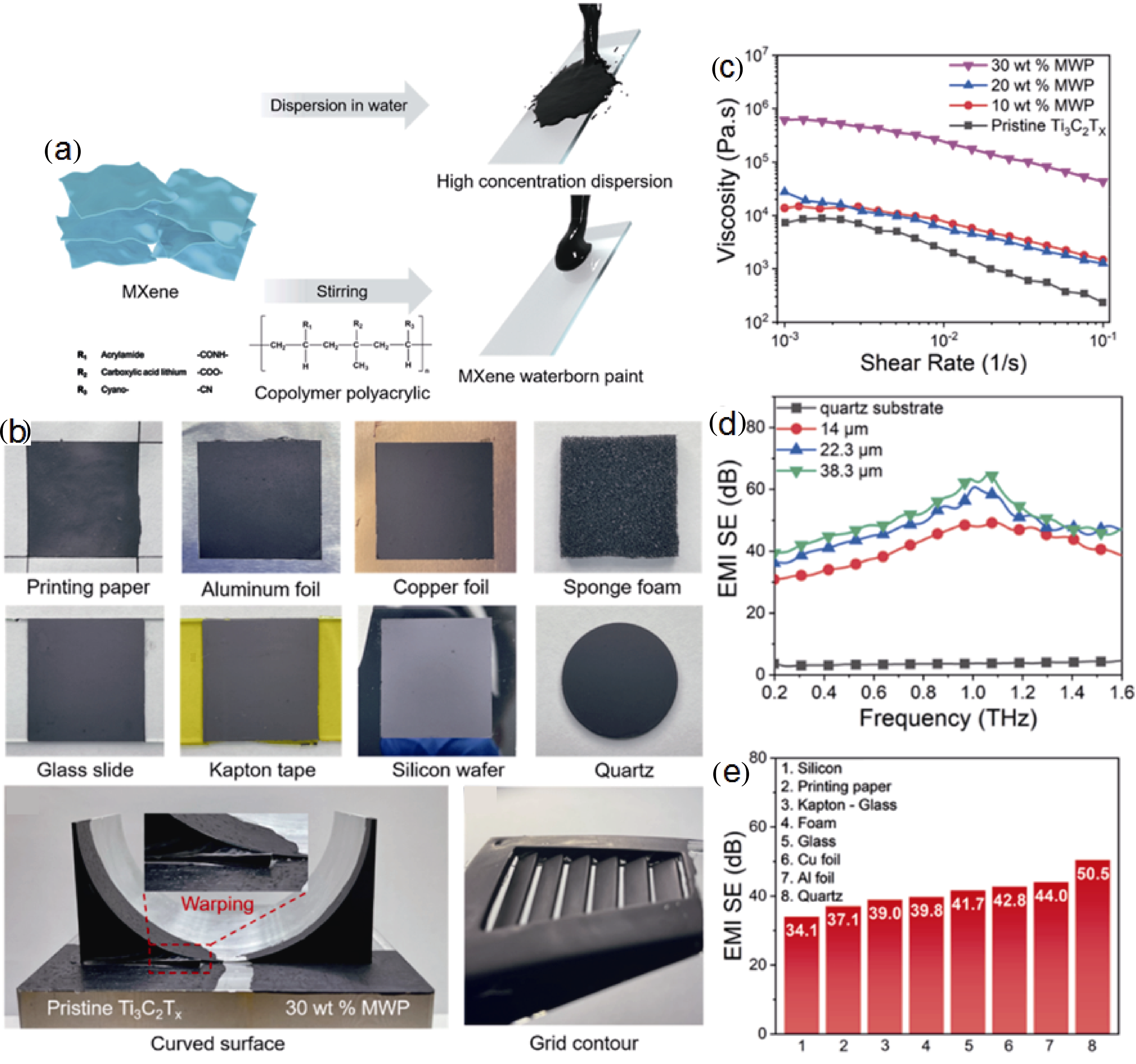
图7 基底普适性Ti3C2Tx复合薄膜涂料(MWP)的制备、黏度及太赫兹电磁屏蔽性能[57]
Fig. 7 Synthesis of MWP, and viscosity and EMI SE measurements of different MXene filler content MWP[57] (a) Schematic of the fabrication of Ti3C2Tx water dispersion and Ti3C2Tx MXene waterborne paint; (b) Photos of 30% MWP coating on different substrates: printing paper, aluminum foil, copper foil, sponge foam, glass slide, Kapton tape, silicon wafer, and quartz; (c) Viscosity of 40 mg·mL−1 MXene water dispersion and MWP with different filler contents; (d) EMI SE versus thickness of 30% MWP on quartz; (e) EMI SE at 1 THz of 30% MWP coated on different types of substrates: flexible, rigid, porous (Reprinted from Ref. [57] with permission, Copyright 2021, American Chemical Society)

图8 利用水氧吸附竞争机制的MXene与层状蒙脱土耐高温太赫兹电磁屏蔽复合薄膜[76]
Fig. 8 High-temperature terahertz electromagnetic shielding composite film of MXene and layered montmorillonite utilizing a water-oxygen adsorption competition mechanism[76] (a) Schematic showing the oxidation process of pristine Ti3C2Tx (starting from the edge) and suppressed oxidation of MEB under high-temperature annealing with the presence of oxygen; (b) Charge density difference plots for the stable configurations of one O2 adsorbed on Ti3C2O2, EB, and Ti3C2O2/EB heterostructure. In the heterostructure, EB is subject to saturated oxygen adsorption. The isosurface level is set to be 0.0002 e/Å3 except for O2 adsorbed on EB with a value of 0.0006 e/Å3. The yellow area indicates charge accumulation, and the green region represents charge depletion; (c) Thermal gravimetric (TG) curves in the air with mass spectrometry analysis (MS) for the atomic mass unit (amu) of 18/H2O and 44/CO2 for Ti3C2Tx and EB (MEB); (d) EMI SE in 0.2-1.3 THz of Ti3C2Tx-Atmos-500C-2, 600C-2, and MEB-Atmos-500C-2, 600C-2; (e) Average THz SE of the samples showed in (d) (Reprinted from Ref. [76] with permission, Copyright 2022, Springer Nature)
| Composition | Density/(g·cm-3) | Thickness/μm | SE/dB | SSE/t/(dB·cm2·g-1) | Absorption /(RL·dB-1) | Frequency band/THz | Ref. | |
|---|---|---|---|---|---|---|---|---|
| Compact & laminated structure | Ti3C2Tx | / | 0.15 | 20 | / | / | 1.0 | [ |
| Ti3C2Tx | ca. 2.39 | 0.025 | ~2.5 | ~7×10⁵ | / | 0.25-2.25 | [ | |
| Ti3C2Tx | / | 25 | 55~70 | / | / | 0.3-0.7 | [ | |
| Ti2CTx/PDMS | / | / | ~6 | / | / | 0.2-3 | [ | |
| PAN/Ti3C2Tx/AgNPs | / | 3.85 | 9.11 | / | / | 0.2-1.2 | [ | |
| Ti3C2Tx/copolymer-polyacrylic | / | 38.3 | 64.9 | / | / | 0.2-1.6 | [ | |
| PVA/Ti3C2Tx/MWCNT | / | 42 | 23~36 | / | / | 0.2-2.0 | [ | |
| Ti3C2Tx/extracted bentonite | / | 11 | 47 | / | / | 0.2-1.3 | [ | |
| Ti3C2Tx/ polyaramids | / | 20 | 52.7 | / | / | 0.2-1.6 | [ | |
| Porous structure | Ti3C2Tx/GO | / | 4000 | / | / | 37 dB | 0.2-2.0 | [ |
| Zn2+/Ti3C2Tx/GO | 0.11 | 85 | 51 | 451.0 | / | 0.2-2.0 | [ | |
| Ti3C2Tx/polyurethane | / | 2000 | / | / | 99.99% | 0.3-1.65 | [ | |
| Ti3C2Tx/PAA/ACC nanoparticle | / | 130 | 45.3 | / | 23.2 | 0.2-2.0 | [ | |
| Ti3C2Tx/polyurethane/SCA/silica | / | 2000 | / | / | 99.6% | 0.3-1.2 | [ | |
| Ti3C2Tx/rGO | / | 148 | ~30 | / | 99.999% | 0.37-2.0 | [ | |
| Ti3C2Tx/polysiloxane | / | 2500 | / | / | 27.3 | 0.2-1.4 | [ |
表3 MXenes及其复合材料的太赫兹电磁屏蔽与吸收特性[57,59,62,76,78⇓⇓⇓⇓⇓⇓⇓⇓⇓⇓ -89]
Table 3 Terahertz electromagnetic shielding and absorption properties of MXenes and their composites [57,59,62,76,78⇓⇓⇓⇓⇓⇓⇓⇓⇓⇓ -89]
| Composition | Density/(g·cm-3) | Thickness/μm | SE/dB | SSE/t/(dB·cm2·g-1) | Absorption /(RL·dB-1) | Frequency band/THz | Ref. | |
|---|---|---|---|---|---|---|---|---|
| Compact & laminated structure | Ti3C2Tx | / | 0.15 | 20 | / | / | 1.0 | [ |
| Ti3C2Tx | ca. 2.39 | 0.025 | ~2.5 | ~7×10⁵ | / | 0.25-2.25 | [ | |
| Ti3C2Tx | / | 25 | 55~70 | / | / | 0.3-0.7 | [ | |
| Ti2CTx/PDMS | / | / | ~6 | / | / | 0.2-3 | [ | |
| PAN/Ti3C2Tx/AgNPs | / | 3.85 | 9.11 | / | / | 0.2-1.2 | [ | |
| Ti3C2Tx/copolymer-polyacrylic | / | 38.3 | 64.9 | / | / | 0.2-1.6 | [ | |
| PVA/Ti3C2Tx/MWCNT | / | 42 | 23~36 | / | / | 0.2-2.0 | [ | |
| Ti3C2Tx/extracted bentonite | / | 11 | 47 | / | / | 0.2-1.3 | [ | |
| Ti3C2Tx/ polyaramids | / | 20 | 52.7 | / | / | 0.2-1.6 | [ | |
| Porous structure | Ti3C2Tx/GO | / | 4000 | / | / | 37 dB | 0.2-2.0 | [ |
| Zn2+/Ti3C2Tx/GO | 0.11 | 85 | 51 | 451.0 | / | 0.2-2.0 | [ | |
| Ti3C2Tx/polyurethane | / | 2000 | / | / | 99.99% | 0.3-1.65 | [ | |
| Ti3C2Tx/PAA/ACC nanoparticle | / | 130 | 45.3 | / | 23.2 | 0.2-2.0 | [ | |
| Ti3C2Tx/polyurethane/SCA/silica | / | 2000 | / | / | 99.6% | 0.3-1.2 | [ | |
| Ti3C2Tx/rGO | / | 148 | ~30 | / | 99.999% | 0.37-2.0 | [ | |
| Ti3C2Tx/polysiloxane | / | 2500 | / | / | 27.3 | 0.2-1.4 | [ |
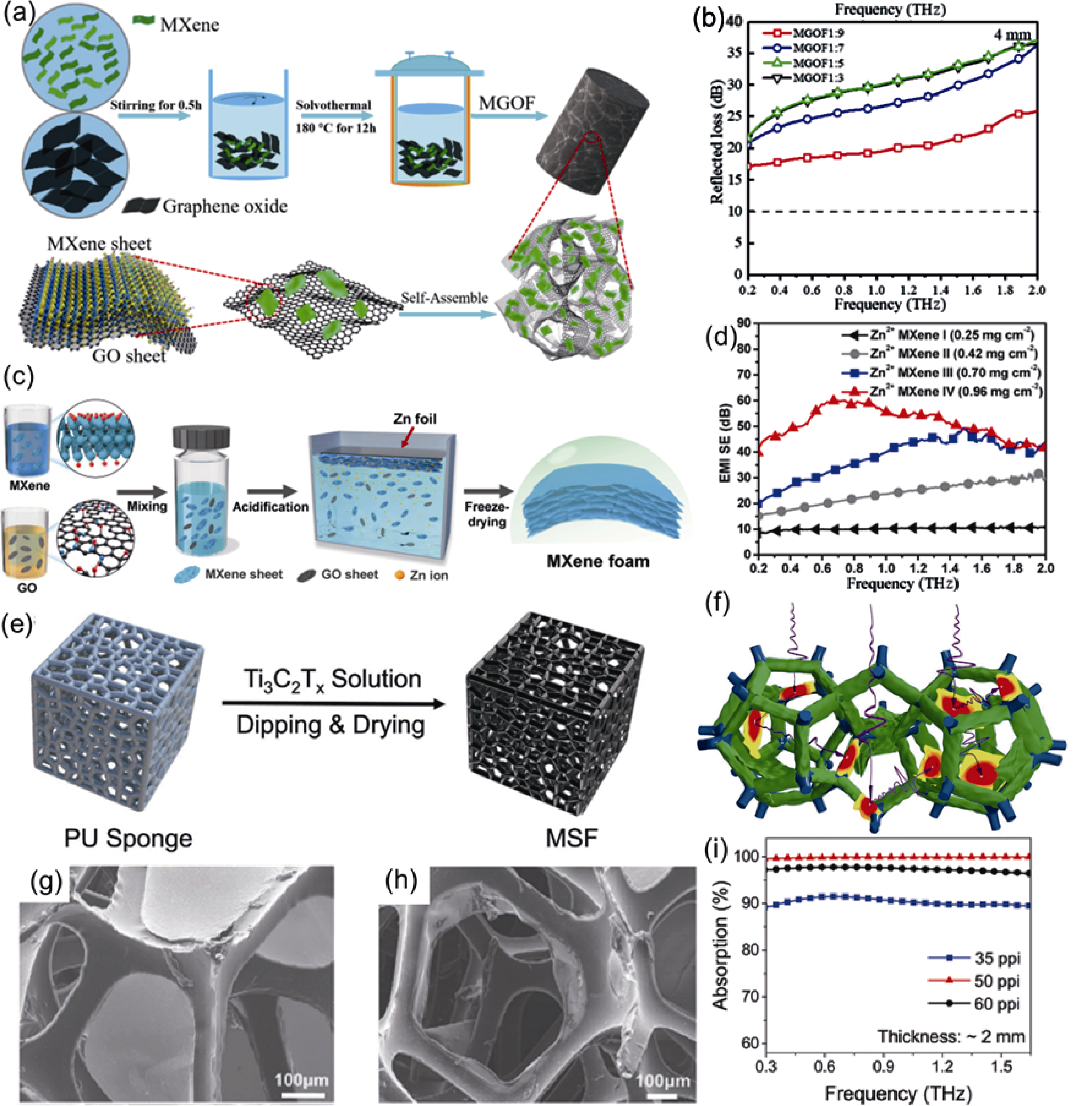
图9 Ti3C2Tx及其复合多孔吸波体的太赫兹吸收特性
Fig. 9 Terahertz absorption characteristics of Ti3C2Tx and its composite porous absorber (a) Schematic diagram of the MXene/GO foam (MGOF) preparation process; (b) RL curves of 4 mm MGOF with different contents of MXene added to the GO foam[83]; (c) Schematic illustrating the ion-diffusion-induced gelation process; (d) THz EMI shielding effectiveness of the Zn2+ MXene-based foams[84]; (e) Schematic illustration of the fabrication of MSF; (f) THz absorption mechanism of MXene filled 3D porous structure with above typical fill state; Two typical filling states: continuous MXene film on pores (g) and/or discontinuous MXene film on skeletons (h); (i) THz absorption by MSF with different pore sizes but fixed 2 mm thickness and (2.8±0.5) mg Ti3C2Tx loading[85] (Reprinted from Ref. [83] and Ref. [84] with permission, Copyright 2019 and 2020, American Chemical Society; Reprinted from Ref. [85] with permission, Copyright 2020, Wiley-VCH GmbH)
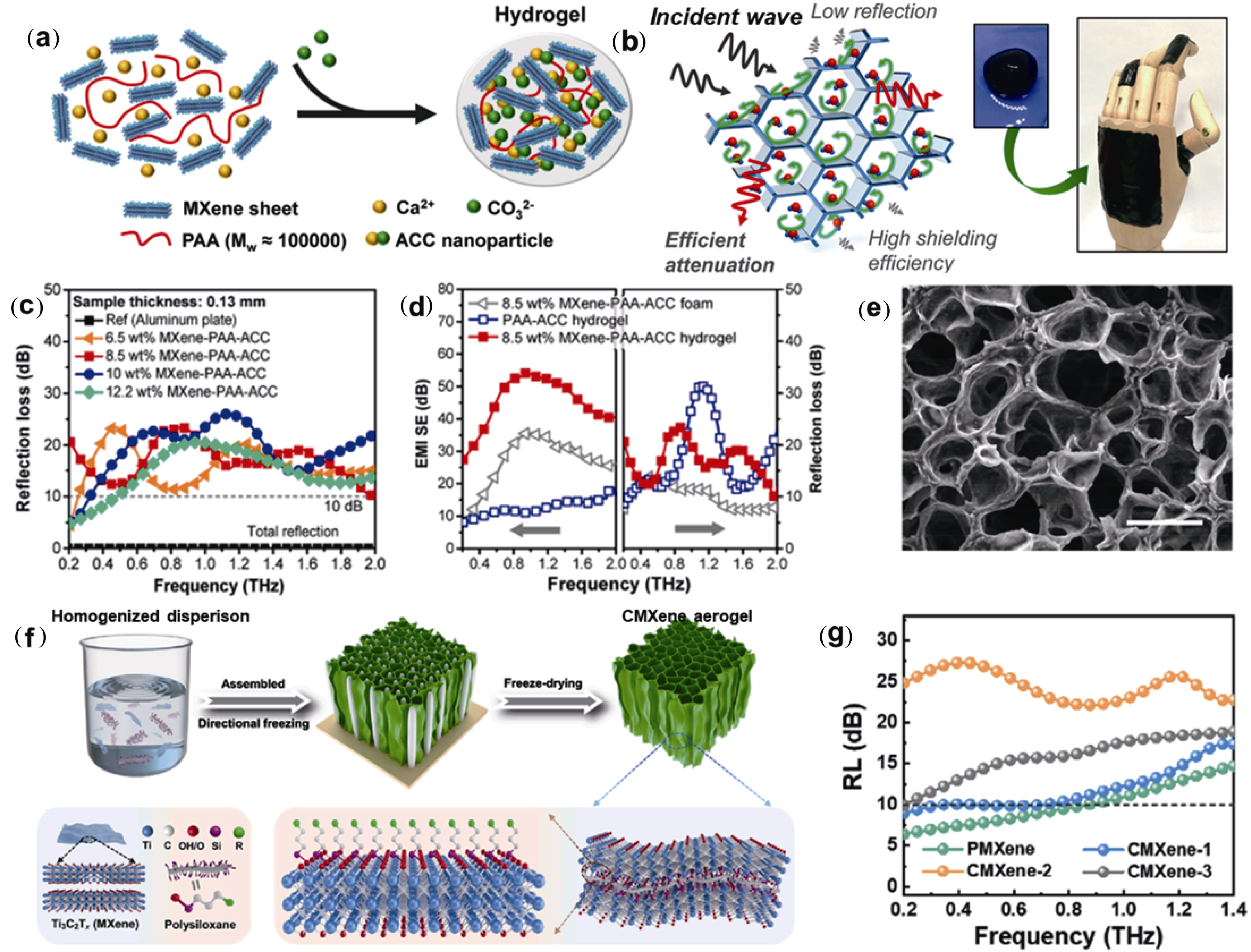
图10 Ti3C2Tx及其复合多孔水凝胶与定向冷冻干燥气凝胶的太赫兹吸收特性
Fig. 10 Terahertz absorption properties of Ti3C2Tx and its composite porous hydrogels and directional freeze-dried aerogels (a) Schematic illustrating the formation of MXene composite hydrogel; (b) Proposed absorption-dominated EMI shielding mechanism of the MXene composite hydrogel; (c) RL curves of MXene composite hydrogels; (d) Comparison of terahertz EMI shielding and absorption performances between MXene composite hydrogel and reference samples; (e) SEM image of MXene composite hydrogel[86]; (f) Schematic illustration of the fabrication of CMXene; (g) RL curves in THz band of all MXene-based absorbers[89] (Reprinted from Ref. [86] with permission, Copyright 2021, American Chemical Society; Reprinted from Ref. [89] with permission, Copyright 2023, Elsevier B.V.)
| [1] |
KULESA C. Terahertz spectroscopy for astronomy: from comets to cosmology. IEEE Transactions on Terahertz Science and Technology, 2011, 1(1): 232.
DOI URL |
| [2] | CHRISTOPHER K. WALKER. Terahertz Astronomy. Boca Raton: Taylor & Francis Group, LLC, 2016: 261-282. |
| [3] |
SENGUPTA K, NAGATSUMA T, MITTLEMAN D M. Terahertz integrated electronic and hybrid electronic-photonic systems. Nature Electronics, 2018, 1(12): 622.
DOI |
| [4] |
LIU J L, DAI J M, CHIN S L, et al. Broadband terahertz wave remote sensing using coherent manipulation of fluorescence from asymmetrically ionized gases. Nature Photonics, 2010, 4(9): 627.
DOI |
| [5] |
BAXTER J B, GUGLIETTA G W. Terahertz spectroscopy. Analytical Chemistry, 2011, 83(12): 4342.
DOI PMID |
| [6] |
SUNG S J, SELVIN S, BAJWA N, et al. THz imaging system for in vivo human cornea. IEEE Transactions on Terahertz Science and Technology, 2018, 8(1): 27.
DOI URL |
| [7] |
YAN Z Y, ZHU L G, MENG K, et al. THz medical imaging: from in vitro to in vivo. Trends in Biotechnology, 2022, 40(7): 816.
DOI URL |
| [8] |
DANG S P, AMIN O, SHIHADA B, et al. What should 6G be? Nature Electronics, 2020, 3(1): 20.
DOI |
| [9] |
RIKKINEN K, KYOSTI P, LEINONEN M E, et al. THz radio communication: link budget analysis toward 6G. IEEE Communications Magazine, 2020, 58(11): 22.
DOI URL |
| [10] |
SERGHIOU D, KHALILY M, BROWN T W C, et al. Terahertz channel propagation phenomena, measurement techniques and modeling for 6G wireless communication applications: a survey, open challenges and future research directions. IEEE Communications Surveys and Tutorials, 2022, 24(4): 1957.
DOI URL |
| [11] |
KUMAR A, GUPTA M, PITCHAPPA P, et al. Phototunable chip- scale topological photonics: 160 Gbps waveguide and demultiplexer for THz 6G communication. Nature Communications, 2022, 13: 5404.
DOI |
| [12] |
YANG Y H, YAMAGAMI Y, YU X B, et al. Terahertz topological photonics for on-chip communication. Nature Photonics, 2020, 14(7): 446.
DOI |
| [13] | JASON F, LARRY S, GASIEWSK A J. A near-millimeter wave interferometric radar. 2013 IEEE Radar Conference, Ottawa, 2013: 1-5. |
| [14] |
ZHANG B, PI Y Y, LI J. Terahertz imaging radar with inverse aperture synthesis techniques: system structure, signal processing, and experiment results. IEEE Sensors Journal, 2015, 15(1): 290.
DOI URL |
| [15] | CARIS M, STANKO S, PALM S, et al. 300 GHz radar for high resolution SAR and ISAR applications. 2015 16th International Radar Symposium (IRS), Dresden, 2015: 577-580. |
| [16] | DICKINSON J C, THOMAS M G, WALDMAN J. High resolution imaging using 325 GHz and 1.5 THz transceivers. 15th International Symposium on Space Terahertz Technology, Northampton, 2004: 373-380. |
| [17] |
HEMMAT M, AYARI S, MIČICA M, et al. Layer-controlled nonlinear terahertz valleytronics in two-dimensional semimetal and semiconductor PtSe2. InfoMat, 2023, 5(11): e12468.
DOI URL |
| [18] |
DONG Z, YU W, ZHANG L, et al. Wafer-scale patterned growth of type-II Dirac semimetal platinum ditelluride for sensitive room- temperature terahertz photodetection. InfoMat, 2023, 5(5): e12403.
DOI URL |
| [19] |
LIU B, ZHANG X, DU J, et al. Synergistic-engineered van der Waals photodiodes with high efficiency. InfoMat, 2022, 4(3): e12282.
DOI URL |
| [20] |
IQBAL A, SAMBYAL P, KOO C M. 2D MXenes for electromagnetic shielding: a review. Advanced Functional Materials, 2020, 30(47): 2000883.
DOI URL |
| [21] |
LIU L, DAS A, MEGARIDIS C M. Terahertz shielding of carbon nanomaterials and their composites—a review and applications. Carbon, 2014, 69: 1.
DOI URL |
| [22] |
CHE R C, PENG L M, DUAN X F, et al. Microwave absorption enhancement and complex permittivity and permeability of Fe encapsulated within carbon nanotubes. Advanced Materials, 2004, 16(5): 401.
DOI URL |
| [23] |
SUN H, CHE R C, YOU X, et al. Cross-stacking aligned carbon- nanotube films to tune microwave absorption frequencies and increase absorption intensities. Advanced Materials, 2014, 26(48): 8120.
DOI URL |
| [24] |
LIU Q H, CAO Q, BI H, et al. CoNi@SiO2@TiO2 and CoNi@Air@TiO2 microspheres with strong wideband microwave absorption. Advanced Materials, 2016, 28(3): 486.
DOI URL |
| [25] |
CHE R C, ZHI C Y, LIANG C Y, et al. Fabrication and microwave absorption of carbon nanotubes/CoFe2O4 spinel nanocomposite. Applied Physics Letters, 2006, 88(3): 033105.
DOI URL |
| [26] |
SOKOL M, NATU V, KOTA S, et al. On the chemical diversity of the MAX phases. Trends in Chemistry, 2019, 1(2): 210.
DOI URL |
| [27] |
DING H M, LI Y B, LI M, et al. Chemical scissor-mediated structural editing of layered transition metal carbides. Science, 2023, 379(6637): 1130.
DOI PMID |
| [28] | WEI Y, ZHANG P, SOOMRO R A, et al. Advances in the synthesis of 2D MXenes. Advanced Materials, 2021, 33(39): e2103148. |
| [29] |
MOHAMMADI A V, ROSEN J, GOGOTSI Y. The world of two-dimensional carbides and nitrides (MXenes). Science, 2021, 372(6547): eabf1581.
DOI URL |
| [30] |
IQBAL A, SHAHZAD F, HANTANASIRISAKUL K, et al. Anomalous absorption of electromagnetic waves by 2D transition metal carbonitride Ti3CNTx (MXene). Science, 2020, 369(6502): 446.
DOI URL |
| [31] |
FAISAL S, MOHAMED A, CHRISTINE B, et al. Electromagnetic interference shielding with 2D transition metal carbides (MXenes). Science, 2016, 353(6304): 1137.
DOI PMID |
| [32] |
WU Z C, CHENG H W, JIN C, et al. Dimensional design and core-shell engineering of nanomaterials for electromagnetic wave absorption. Advanced Materials, 2022, 34(11): 2107538.
DOI URL |
| [33] |
LU J, LI X, HWANG H Y, et al. Coherent two-dimensional terahertz magnetic resonance spectroscopy of collective spin waves. Physical Review Letters, 2017, 118(20): 207204.
DOI URL |
| [34] |
CASPERS C, GANDHI V P, MAGREZ A, et al. Sub-terahertz spectroscopy of magnetic resonance in BiFeO3 using a vector network analyzer. Applied Physics Letters, 2016, 108(24): 241109.
DOI URL |
| [35] |
BITZER A, MERBOLD H, THOMAN A, et al. Terahertz near-field imaging of electric and magnetic resonances of a planar metamaterial. Optics Express, 2009, 17(5): 3826.
PMID |
| [36] |
YEN T J, PADILLA W J, FANG N, et al. Terahertz magnetic response from artificial materials. Science, 2004, 303(5663): 1494.
PMID |
| [37] |
WATTS C M, LIU X L, PADILLA W J. Metamaterial electromagnetic wave absorbers. Advanced Materials, 2012, 24(23): 98.
DOI |
| [38] | YOUJI K. Electromagnetic wave absorbers detailed theories and applications. Hoboken: John Wiley & Sons, Inc, 2019: 5-20. |
| [39] | SALISBURY W W. Absorbent body for electromagnetic waves. US2599944. 1952-06-10. |
| [40] | LI H, LI F F, FAN D G, et al. Wideband electromagnetic absorber based on array of parallel-plate waveguide. 2017 International Conference on Electromagnetics in Advanced Applications (Iceaa), 2017: 1224-1226. |
| [41] |
COSTA F, MONORCHIO A. A frequency selective radome with wideband absorbing properties. IEEE Transactions on Antennas and Propagation, 2012, 60(6): 2740.
DOI URL |
| [42] |
JI B, FAN S W, KOU S J, et al. Microwave absorption properties of multilayer impedance gradient absorber consisting of Ti3C2Tx MXene/polymer films. Carbon, 2021, 181: 130.
DOI URL |
| [43] |
ZUO Y X, SU X R, LI X W, et al. Multimaterial 3D-printing of graphene/LiZnFeO and graphene/carbonyl iron composites with superior microwave absorption properties and adjustable bandwidth. Carbon, 2020, 167: 62.
DOI URL |
| [44] |
DEWITT B T, BURNSIDE W D. Electromagnetic scattering by pyramidal and wedge absorber. IEEE Transactions on Antennas and Propagation, 1988, 36(7): 971.
DOI URL |
| [45] |
JOHNK R T, ONDREJKA A, TOFANI S, et al. Time-domain measurements of the electromagnetic backscatter of pyramidal absorbers and metallic plates. IEEE Transactions on Electromagnetic Compatibility, 1993, 35(4): 429.
DOI URL |
| [46] |
SHEN Z, LI S, XU Y, et al. Three-dimensional printed ultrabroadband terahertz metamaterial absorbers. Physical Review Applied, 2021, 16(1): 014066.
DOI URL |
| [47] |
WANG C Q, SWEENEY W R, STONE A D, et al. Coherent perfect absorption at an exceptional point. Science, 2021, 373(6560): 1261.
DOI PMID |
| [48] |
SLOBODKIN Y, WEINBERG G, HORNER H, et al. Massively degenerate coherent perfect absorber for arbitrary wavefronts. Science, 2022, 377(6609): 995.
DOI PMID |
| [49] |
BARANOV D G, KRASNOK A, SHEGAI T, et al. Coherent perfect absorbers: linear control of light with light. Nature Reviews Materials, 2017, 2(12): 17064.
DOI URL |
| [50] |
LI S C, LUO J, ANWAR S, et al. Broadband perfect absorption of ultrathin conductive films with coherent illumination: superabsorption of microwave radiation. Physical Review B, 2015, 91(22): 220301.
DOI URL |
| [51] | PAPAIOANNOU M, PLUM E, VALENTE J, et al. Two-dimensional control of light with light on metasurfaces. Light-Science & Applications, 2016, 5: e16070. |
| [52] |
NARIMANOV E E, KILDISHEV A V. Optical black hole: broadband omnidirectional light absorber. Applied Physics Letters, 2009, 95(4): 041106.
DOI URL |
| [53] | LEONARD M H, KEITH A S. Integrating spheres for mid- and near infrared reflection spectroscopy. Chichester: John Wiley & Sons Ltd, 2002. |
| [54] |
WANG C L, CHIU C P, HUANG P J, et al. High-performance 1-10 THz integrating sphere. Applied Optics, 2021, 60(13): 3784.
DOI URL |
| [55] | WU Y, BAI Y. Radar cross section measurement in terahertz. 2016 Progress in Electromagnetics Research Symposium (Piers), 2016: 2991-2994. |
| [56] |
IWASZCZUK K, HEISELBERG H, JEPSEN P U. Terahertz radar cross section measurements. Optics Express, 2010, 18(25): 26399.
DOI PMID |
| [57] |
WAN H J, LIU N, TANG J, et al. Substrate-independent Ti3C2Tx MXene waterborne paint for Terahertz absorption and shielding. ACS Nano, 2021, 15(8): 13646.
DOI URL |
| [58] |
JHON Y I, SEO M, JHON Y M. First-principles study of a MXene terahertz detector. Nanoscale, 2018, 10(1): 69.
DOI URL |
| [59] |
CHOI G, SHAHZAD F, BAHK Y M, et al. Enhanced terahertz shielding of MXenes with nano-metamaterials. Advanced Optical Materials, 2018, 6(5): 1701076.
DOI URL |
| [60] | LI G J, KUSHNIR K, DONG Y C, et al. Equilibrium and non-equilibrium free carrier dynamics in 2D Ti3C2Tx MXenes: THz spectroscopy study. 2D Materials, 2018, 5(3): 035043. |
| [61] |
LUI G, NATU V, SHI T, et al. Two-dimensional MXenes Mo2Ti2C3Tz and Mo2TiC2Tz: microscopic conductivity and dynamics of photoexcited carriers. ACS Applied Energy Materials, 2020, 3(2): 1530.
DOI URL |
| [62] |
LI G J, AMER N, HAFEZ H A, et al. Dynamical control over Terahertz electromagnetic interference shielding with 2D Ti3C2Ty MXene by ultrafast optical pulses. Nano Letters, 2020, 20(1): 636.
DOI URL |
| [63] | COLIN-ULLOA E, FITZGERALD A, MONTAZERI K, et al. Ultrafast spectroscopy of plasmons and free carriers in 2D MXenes. Advanced Materials, 2023, 35(8): e2208659. |
| [64] |
ZHENG W, SUN B, LI D, et al. Band transport by large Fröhlich polarons in MXenes. Nature Physics, 2022, 18(5): 544.
DOI |
| [65] |
ZHAO T, XIE P Y, WAN H J, et al. Ultrathin MXene assemblies approach the intrinsic absorption limit in the 0.5-10 THz band. Nature Photonics, 2023, 17(7): 622.
DOI |
| [66] |
LI Y B, SHAO H, LIN Z F, et al. A general Lewis acidic etching route for preparing MXenes with enhanced electrochemical performance in non-aqueous electrolyte. Nature Materials, 2020, 19(8): 894.
DOI PMID |
| [67] |
MATHIS T S, MALESKI K, GOAD A, et al. Modified MAX phase synthesis for environmentally stable and highly conductive Ti3C2 MXene. ACS Nano, 2021, 15(4): 6420.
DOI URL |
| [68] |
KIM Y J, KIM S J, SEO D, et al. Etching mechanism of monoatomic aluminum layers during MXene synthesis. Chemistry of Materials, 2021, 33(16): 6346.
DOI URL |
| [69] |
MICHALOWSKI P P, ANAYEE M, MATHIS T S, et al. Oxycarbide MXenes and MAX phases identification using monoatomic layer-by-layer analysis with ultralow-energy secondary-ion mass spectrometry. Nature Nanotechnology, 2022, 17(11): 1192.
DOI |
| [70] |
BALCI O, POLAT E O, KAKENOV N, et al. Graphene-enabled electrically switchable radar-absorbing surfaces. Nature Communications, 2015, 6: 6628.
DOI PMID |
| [71] |
PHAM P H Q, ZHANG W D, QUACH N V, et al. Broadband impedance match to two-dimensional materials in the terahertz domain. Nature Communications, 2017, 8: 2233.
DOI PMID |
| [72] |
STEN J C E, KOIVISTO P K. Optimum transparent absorbers of electromagnetic waves. IEEE Transactions on Electromagnetic Compatibility, 2008, 50(4): 1011.
DOI URL |
| [73] | THOMASSIN J M, JEROME C, PARDOEN T, et al. Polymer/ carbon based composites as electromagnetic interference (EMI) shielding materials. Materials Science & Engineering R-Reports, 2013, 74(7): 2112. |
| [74] |
OLIVEIRA F M, AZADMANJIRI J, WANG X H, et al. Structure design and processing strategies of MXene-based materials for electromagnetic interference shielding. Small Methods, 2023, 7(7): 2300112.
DOI URL |
| [75] |
WAN S J, LI X, CHEN Y, et al. High-strength scalable MXene films through bridging-induced densification. Science, 2021, 374(6563): 96.
DOI PMID |
| [76] |
LIU N, LI Q Q, WAN H J, et al. High-temperature stability in air of Ti3C2Tx MXene-based composite with extracted bentonite. Nature Communications, 2022, 13: 5551.
DOI |
| [77] | FENG T D, HU Y W, CHANG X, et al. Highly flexible Ti3C2Tx MXene/waterborne polyurethane membranes for high-efficiency terahertz modulation with low insertion loss. ACS Applied Materials & Interfaces, 2023, 15(5): 7592. |
| [78] |
ZOU Q, GUO W Y, ZHANG L, et al. MXene-based ultra-thin film for terahertz radiation shielding. Nanotechnology, 2020, 31(50): 505710.
DOI |
| [79] |
KLAUDIA Z A L, AGNIESZKA S, AGNIESZKA M, et al. Terahertz time domain spectroscopy of graphene and MXene polymer composites. Journal of Applied Polymer Science, 2020, 138(10): 49962
DOI URL |
| [80] |
ZOU Q, SHI C F, LIU B, et al. Enhanced terahertz shielding by adding rare Ag nanoparticles to Ti3C2Tx MXene fiber membranes. Nanotechnology, 2021, 32(41): 415204.
DOI |
| [81] |
HUSSAIN K, MEHBOOB S, AHMAD I, et al. Terahertz time- domain spectroscopy of thin and flexible CNT-modified MXene/ polymer composites. Applied Physics A, 2021, 127(5): 382.
DOI |
| [82] |
CHENG Z, CAO Y, WANG R, et al. Multifunctional MXene-based composite films with simultaneous terahertz/gigahertz wave shielding performance for future 6G communication. Journal of Materials Chemistry A, 2023, 11(11): 5593.
DOI URL |
| [83] | MA W L, CHEN H H, HOU S Y, et al. Compressible highly stable 3D porous MXene/GO foam with a tunable high-performance stealth property in the terahertz band. ACS Applied Materials & Interfaces, 2019, 11(28): 25369. |
| [84] |
LIN Z H, LIU J, PENG W, et al. Highly stable 3D Ti3C2Tx MXene-based foam architectures toward high-performance terahertz radiation shielding. ACS Nano, 2020, 14(2): 2109.
DOI URL |
| [85] |
SHUI W C, LI J M, WANG H, et al. Ti3C2Tx MXene sponge composite as broadband terahertz absorber. Advanced Optical Materials, 2020, 8(21): 2001120.
DOI URL |
| [86] |
ZHU Y Y, LIU J, GUO T, et al. Multifunctional Ti3C2Tx MXene composite hydrogels with strain sensitivity toward absorption- dominated electromagnetic-interference shielding. ACS Nano, 2021, 15(1): 1465.
DOI URL |
| [87] |
LUO M, GUO J C, SHUI W C, et al. Ti3C2Tx MXene-based superhydrophobic broadband terahertz absorber with large pore-size foam architecture. Advanced Materials Interfaces, 2022, 10(2): 2201767.
DOI URL |
| [88] |
LI S J, XU S J, PAN K C, et al. Ultra-thin broadband terahertz absorption and electromagnetic shielding properties of MXene/ rGO composite film. Carbon, 2022, 194: 127.
DOI URL |
| [89] |
FEI Y, WANG X Y, WANG F, et al. Covalent coupling induced-polarization relaxation in MXene-based terahertz absorber for realizing dual band absorption. Chemical Engineering Journal, 2023, 461: 142049.
DOI URL |
| [90] |
WANG L, MA Z, ZHANG Y, et al. Polymer-based EMI shielding composites with 3D conductive networks: a mini-review. SusMat, 2021, 1(3): 413.
DOI URL |
| [91] |
HORODYNSKI M, KUHMAYER M, FERISE C, et al. Anti- reflection structure for perfect transmission through complex media. Nature, 2022, 607(7918): 281.
DOI |
| [92] |
YUN T, LEE G S, CHOI J, et al. Multidimensional Ti3C2Tx MXene architectures via interfacial electrochemical self-assembly. ACS Nano, 2021, 15(6): 10058.
DOI URL |
| [93] |
XUE T T, YANG Y, YU D Y, et al. 3D printed integrated gradient-conductive MXene/CNT/polyimide aerogel frames for electromagnetic interference shielding with ultra-low reflection. Nano-Micro Letters, 2023, 15(1): 45.
DOI PMID |
| [1] | 李雷, 程群峰. 高性能MXenes纳米复合材料研究进展[J]. 无机材料学报, 2024, 39(2): 153-161. |
| [2] | 徐向明, Husam N ALSHAREEF. MXetronics—MXene电子学[J]. 无机材料学报, 2024, 39(2): 171-178. |
| [3] | 李腊, 沈国震. 二维MXenes材料在柔性光电探测器中的应用展望[J]. 无机材料学报, 2024, 39(2): 186-194. |
| [4] | 巴坤, 王建禄, 韩美康. MXene的红外特性及其应用研究展望[J]. 无机材料学报, 2024, 39(2): 162-170. |
| [5] | 尹建宇, 刘逆霜, 高义华. MXene在压力传感中的研究进展[J]. 无机材料学报, 2024, 39(2): 179-185. |
| [6] | 刘艳艳, 谢曦, 刘增乾, 张哲峰. MAX相陶瓷增强金属基复合材料: 制备、性能与仿生设计[J]. 无机材料学报, 2024, 39(2): 145-152. |
| [7] | 邓顺桂, 张传芳. 多功能MXene油墨:面向印刷能源及电子器件的新视角[J]. 无机材料学报, 2024, 39(2): 195-203. |
| [8] | 陈泽, 支春义. MXene在锌离子电池中的应用: 研究进展与展望[J]. 无机材料学报, 2024, 39(2): 204-214. |
| [9] | 丁浩明, 陈科, 李勉, 李友兵, 柴之芳, 黄庆. 无机材料的“化学剪刀”结构编辑策略[J]. 无机材料学报, 2024, 39(2): 115-128. |
| [10] | 费玲, 雷蕾, 汪德高. 二维MXene材料在新型薄膜太阳能电池技术中的研究进展[J]. 无机材料学报, 2024, 39(2): 215-224. |
| [11] | 陶顺衍, 杨加胜, 邵芳, 吴应辰, 赵华玉, 董绍明, 张翔宇, 熊瑛. 航机CMC热端部件用热喷涂涂层的机遇与挑战[J]. 无机材料学报, 2024, 39(10): 1077-1083. |
| [12] | 郑嘉乾, 卢霄, 鲁亚杰, 王迎军, 王臻, 卢建熙. 医用生物陶瓷的功能性生物适配机制及应用[J]. 无机材料学报, 2024, 39(1): 1-16. |
| [13] | 孙晗, 李文俊, 贾子璇, 张岩, 殷利迎, 介万奇, 徐亚东. ACRT技术对大尺寸ZnTe晶体溶液法制备及其性能影响[J]. 无机材料学报, 2023, 38(3): 310-315. |
| [14] | 李涛, 曹鹏飞, 胡力涛, 夏勇, 陈一, 刘跃军, 孙翱魁. NH4+扩层MoS2的制备及其储锌性能研究[J]. 无机材料学报, 2023, 38(1): 79-86. |
| [15] | 孙炼, 顾全超, 杨雅萍, 王洪磊, 余金山, 周新贵. 二维过渡金属硫属化合物氧还原反应催化剂的研究进展[J]. 无机材料学报, 2022, 37(7): 697-709. |
| 阅读次数 | ||||||||||||||||||||||||||||||||||||||||||||||||||
|
全文 627
|
|
|||||||||||||||||||||||||||||||||||||||||||||||||
|
摘要 702
|
|
|||||||||||||||||||||||||||||||||||||||||||||||||